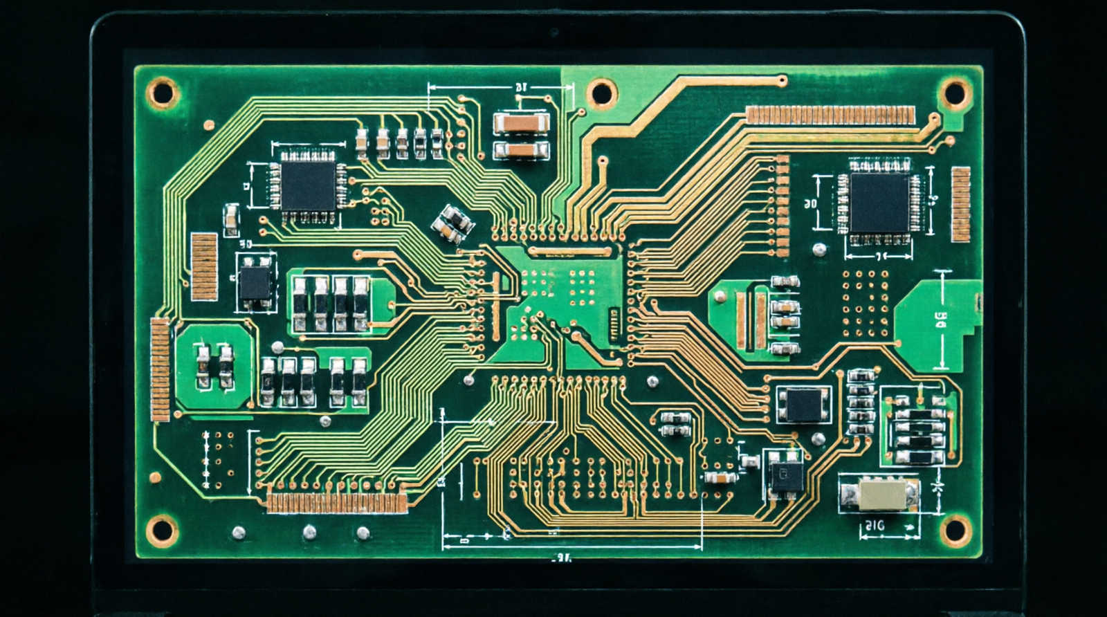
Modern PCB design requires precision at every stage - from schematic to final assembly
Why PCB Design Excellence Matters
A well-designed PCB is the foundation of every reliable electronic product. At BenDeb Creations, we've designed hundreds of boards for IoT solutions, smart devices, and embedded systems. The difference between a product that works flawlessly for years and one that fails in the field often comes down to decisions made in the first hours of design.
Whether you're developing a prototype or scaling to production, these proven practices will save you time, reduce costs, and prevent costly redesigns.
📐 Phase 1: Schematic Design - Your Single Source of Truth
The schematic is where every successful PCB begins. Resist the temptation to jump straight to layout—investing time in a clean, logical schematic pays dividends throughout your entire project lifecycle.
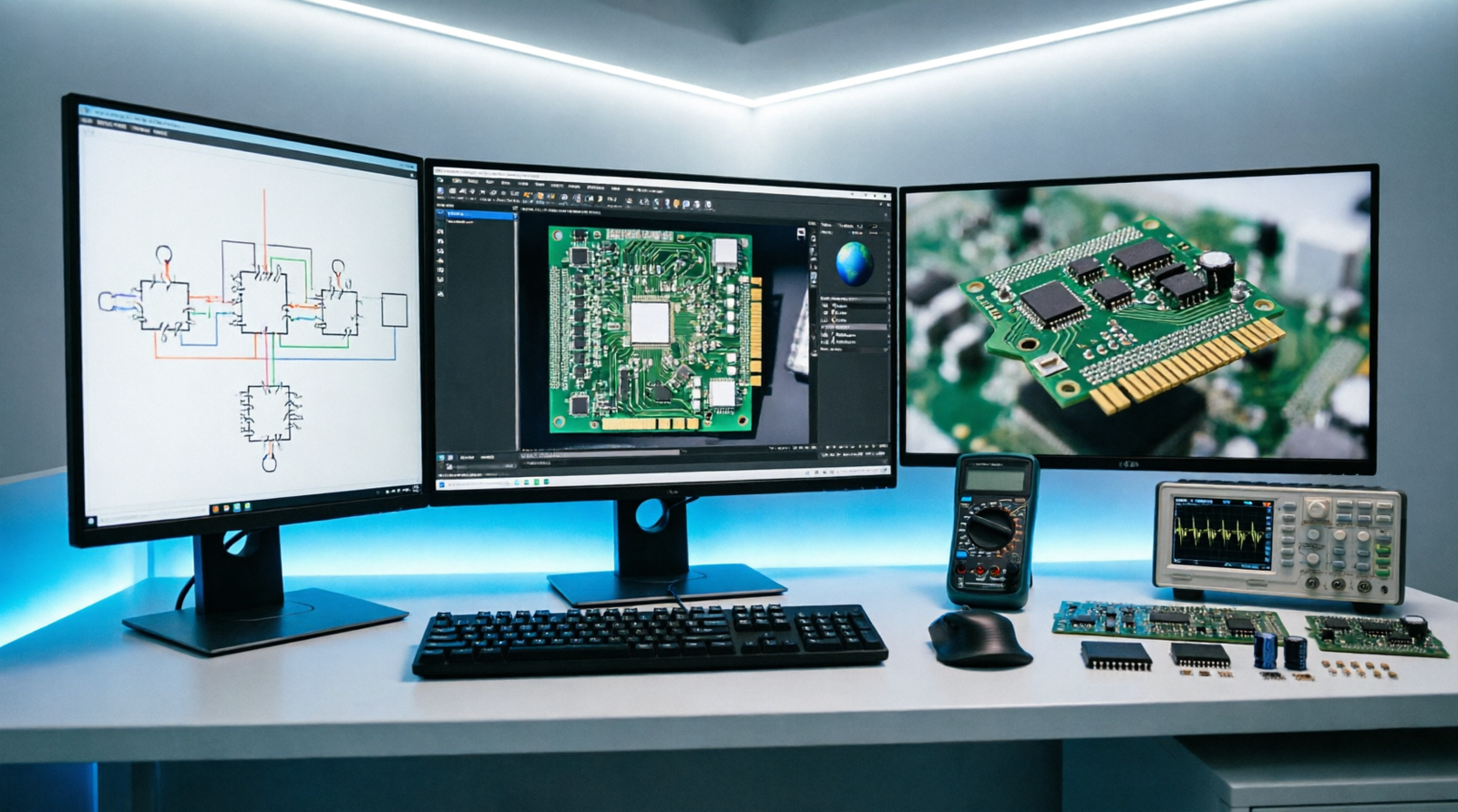
Professional EDA tools like Altium Designer and KiCad provide powerful schematic capture capabilities
Essential Schematic Practices
- Use Hierarchical Design: Break complex designs into logical sheets—power management, MCU core, communication interfaces (I2C, SPI, UART), and sensor modules. This improves readability and makes debugging easier.
- Decoupling Strategy: Place decoupling capacitors at every IC power pin. Use 100nF ceramic capacitors for high-frequency noise suppression and 10µF tantalum or ceramic for bulk capacitance. Place them as close as possible to the power pins.
- Test Points Everywhere: Add test points for all power rails (3.3V, 5V, VBAT), ground references, reset lines, and critical signals. You'll thank yourself during bring-up and debugging.
- Comprehensive Labeling: Use descriptive net labels (not just "Net1", "Net2"). Label connectors with pin functions. Add comments explaining non-obvious design choices.
- ERC Before Layout: Run Electrical Rule Check religiously. Fix every warning, even the ones that seem harmless.
💡 BenDeb Pro Tip
- Create a standardized schematic template with your company logo, common symbols, and pre-configured title blocks
- Use off-page connectors consistently to make signal flow obvious
- Document design decisions directly in the schematic notes
🔧 Phase 2: Strategic Component Selection
Component selection can make or break your project's timeline and budget. That exciting new chip you found might have a 52-week lead time or be discontinued next quarter.
Selection Criteria for Production-Ready Designs
| Factor | Prototype | Production |
|---|---|---|
| Availability | In stock at DigiKey/Mouser | Multiple suppliers, 12+ month lifecycle |
| Lead Time | Same-day shipping OK | Standard lead time < 12 weeks |
| Package | Hand-solderable (SOIC, QFP) | Assembly-friendly (QFN, BGA with proper pitch) |
| Cost | Unit price acceptable | Volume pricing at 1k+ units |
| Documentation | Basic datasheet | Complete reference designs, IBIS models |
Pro Tip from BenDeb: Check the manufacturer's PCN (Product Change Notification) history before committing to a component. Parts with frequent changes cause supply chain headaches and may require redesigns mid-production.
🎨 Phase 3: PCB Layout - Where Art Meets Engineering
Layout is where your schematic becomes a physical reality. Good layout balances electrical performance, manufacturability, and mechanical constraints.

Strategic component placement and routing are critical for signal integrity and EMI performance
1. Component Placement Strategy
Placement determines 80% of your routing success. Follow these principles:
- Functional Grouping: Keep related circuits together—MCU near its crystal and flash memory, power regulation near the input connector, sensors near their mechanical interfaces.
- Signal Flow: Arrange components to follow the natural signal flow from input to output. This minimizes trace crossings and simplifies routing.
- High-Frequency First: Place high-speed components (crystals, RF modules, high-speed interfaces) first, keeping their traces as short as possible.
- Thermal Considerations: Position heat-generating components (voltage regulators, power MOSFETs) with adequate airflow and copper area for heat dissipation.
- Mechanical Constraints: Respect keep-out zones for mounting holes, connectors, and enclosure features. Consider connector orientation for cable routing.
2. Ground Plane Architecture
A solid ground strategy is non-negotiable for reliable designs, especially mixed-signal IoT devices:
- 4-Layer Stackup: For designs with signals above 50MHz or sensitive analog circuits, use: Signal → GND → Power → Signal
- Continuous Ground: Maintain an unbroken ground plane under high-speed signals. Avoid splits or slots that force return currents to take long paths.
- Analog/Digital Separation: For mixed-signal designs, use separate analog and digital ground planes connected at a single point (usually under the ADC/DAC).
- Via Stitching: Place ground vias every 1-2cm around the board perimeter and near high-speed signal vias to provide return current paths.
3. Trace Routing Best Practices
Route critical signals first, then power, then everything else:
- Use 45° angles or curved traces—never 90° bends on high-speed lines (causes impedance discontinuities)
- Maintain consistent trace width for impedance-controlled lines (USB, HDMI, DDR)
- Route differential pairs together with matched lengths (±5mil for USB, ±10mil for Ethernet)
- Keep clock traces short and avoid routing near board edges or noisy circuits
- Daisy-chaining decoupling capacitors instead of connecting each directly to the power pin
- Running high-speed traces over ground plane splits
- Insufficient clearance between high-voltage and low-voltage circuits
- Forgetting to add thermal reliefs on power connections to large copper areas
🏭 Phase 4: Design for Manufacturing (DFM)
Before sending your design to the fab, run comprehensive DFM checks. Most manufacturers provide free DFM analysis tools.

Modern PCB fabrication requires strict adherence to manufacturing tolerances
DFM Checklist
- Trace/Space: Minimum 0.15mm (6mil) for most fabs; 0.1mm (4mil) for advanced processes
- Drill Sizes: Minimum 0.3mm (12mil) for standard; 0.2mm (8mil) adds cost
- Annular Ring: Minimum 0.15mm around drill holes
- Copper-to-Edge: Keep 0.5mm clearance from board edge
- Silkscreen: No text on pads, minimum 0.15mm line width, 6pt font minimum
- Solder Mask: Verify dam between fine-pitch BGA pads (0.1mm minimum)
- Panelization: Add tooling holes and breakaway tabs for panel fabrication
Assembly Considerations (DFA)
- Component Spacing: Minimum 0.5mm between components for reflow soldering
- Fiducials: Add 3 global fiducials (1-2mm diameter) for pick-and-place machines
- Panel Rails: Leave 5-10mm edge clearance for conveyor rails
- Component Height: Verify clearance with enclosure and connectors
🧪 Phase 5: Testing & Validation
Never skip testing. A systematic validation process catches issues before they become field failures.
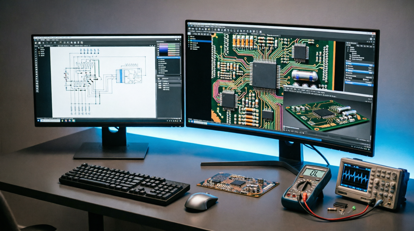
Comprehensive testing at every stage ensures product reliability
Testing Protocol
- Visual Inspection: Check for solder bridges, cold joints, and component orientation
- Power-Off Tests:
- Continuity check on power nets (no shorts)
- Diode test on power rails
- Verify ground connections
- Bring-Up Sequence:
- Apply power with current limiting (start at 100mA)
- Verify all voltage rails (3.3V, 5V, 1.8V, etc.)
- Check for excessive current draw
- Monitor for hot spots with thermal camera
- Functional Testing:
- MCU bootloader and programming
- Clock signals and reset circuits
- Communication interfaces (I2C, SPI, UART)
- Sensor calibration and verification
- Wireless connectivity (WiFi, Bluetooth, LoRa)
- Environmental Testing:
- Thermal cycling (-20°C to +70°C for industrial)
- Vibration testing for mobile applications
- Humidity testing (85°C/85% RH)
- EMC Pre-Compliance:
- Radiated emissions scan (if you have access to a chamber)
- ESD testing (±8kV contact, ±15kV air)
- Fast transient burst immunity
❌ Common Pitfalls & How to Avoid Them
After designing hundreds of boards at BenDeb Creations, here are the mistakes we see most often:
- Missing Bootloader Configuration: Always verify your MCU can be programmed in-circuit. Include SWD/JTAG headers and boot mode jumpers.
- Incorrect Footprints: Always verify pad dimensions against the manufacturer's datasheet—not just the package name. A "0603" from one vendor might differ from another.
- Floating Pins: I2C pull-ups, reset lines, unused MCU pins, and boot configuration pins all need proper termination. Don't leave them floating.
- Insufficient Test Access: You WILL need to probe signals during debugging. Add test points for critical nets, even if they're not in the final product.
- Power Budget Miscalculation: Calculate worst-case current draw for each rail. Size traces and regulators accordingly with 30% headroom.
- Ignoring ESD Protection: Add TVS diodes on all external connectors (USB, Ethernet, buttons). A $0.10 component can save a $50 board.
- No Version Control: Use Git or your EDA's version control. Document every change. "What changed between rev A and rev B?" should never be a mystery.
Documentation & Handoff
Professional designs require professional documentation:
- Gerber Files: RS-274X format with embedded aperture definitions
- Drill Files: Excellon format with tool list
- BOM: Complete with MPN, manufacturer, quantity, and reference designators
- Assembly Drawings: Top/bottom views with component outlines
- Test Procedures: Step-by-step bring-up and functional test instructions
- Design Notes: Known issues, workarounds, and special considerations
🎯 The BenDeb Creations Difference
We specialize in taking your IoT and smart device concepts from prototype to production. Our expertise spans:
- ✓ PCB Design & Layout for IoT, embedded systems, and smart devices
- ✓ Microcontroller Programming (ARM, AVR, ESP32, STM32)
- ✓ Wireless Connectivity (WiFi, Bluetooth, LoRa, Zigbee)
- ✓ Product Management & Agile Development
- ✓ Manufacturing Support & Supply Chain Optimization
🚀 Ready to Bring Your Product to Life?
Whether you're designing your first PCB or scaling to production, BenDeb Creations is here to help. We've guided dozens of startups and established companies through the complexities of PCB design, from initial concept to manufacturing.
Get expert guidance on:
- Schematic review and optimization
- PCB layout for signal integrity and EMI compliance
- Component selection and supply chain management
- DFM/DFA analysis and manufacturing handoff
- Testing strategies and validation protocols
📞 Prefer to talk? Reach out to discuss your project requirements
We typically respond within 24 hours
© 2026 BenDeb Creations. Specializing in Smart Technology, IoT Solutions, and Embedded Systems Development. All rights reserved.